What Is an Analog to Digital Converter?
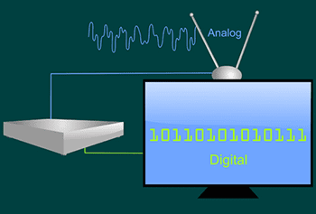
As the name implies, an analog to digital converter (ADC) is an electronic device that converts continuous time-varying analog impulses into discrete-time digital signals that can be read readily by digital devices. It can be used in various electronic projects. ADC translates real-world physical quantities into a digital language that is utilized in control systems, data computing, data transfer, and information processing. An Analogue to Digital Converter, or ADC, is a data converter that converts an analogue signal into a binary code, allowing digital circuitry to interact with the real world.
Microprocessor-controlled circuits, Arduinos, Raspberry Pis, and other digital logic circuits need Analogue-to-Digital Converters (ADCs) to connect with the outside world. Many digital systems interact with the environment by measuring the analogue signals from such transducers. In the real world/situations, analogue signals have continuously changing values that come from various sources and sensors that can measure sound, temperature, light, or movement, and many digital systems interact with the environment by measuring the analogue signals from such transducers.
When it comes to working with digital systems that communicate with real-time signals, analog-to-digital converters (ADCs) are critical components. With the Internet of Things (IoT) rapidly becoming part of everyday life, these digital devices have to be able to interpret real-world/time signals in order to reliably offer crucial information.
We’ll look at how ADCs function and the theory behind them.
How ADCs Work
Analog signals are signals that have a continuous sequence with continuous values in the real world (there are cases where it can be finite). Sound, light, temperature, and motion are all examples of these types of signals. The signal is broken into sequences that rely on the time series or sampling rate, while with a sequence of discrete values digital signals are represented.
Values can’t be read by microcontrollers unless they’re digital data. This is because micro controllers can only see “levels” of voltage, which are determined by the ADC’s resolution and the system voltage.
When converting analog signals to digital, ADCs follow a set of steps. They sample the signal, then quantify it to establish the signal’s resolution before setting binary values and sending it to the system to read the digital signal.
An ADC samples an analog waveform at regular intervals and assigns each sample a digital value. In a binary code format, the digital value displays on the converter’s output. Divide the sampled analog input voltage by the reference voltage, then multiply by the number of digital codes to get the value. The amount of binary bits in the output code determines the converter’s resolution.
The sampling and quantization steps are carried out using an ADC. An analog signal with infinite resolution is represented by the ADC as a digital code with finite resolution. The ADC generates two digital values, with N denoting the number of binary output bits. Because the converter has finite resolution, the analog input signal will lie between the quantization levels, resulting in intrinsic uncertainty or quantization error. The maximum dynamic range of the converter is determined by this mistake.
A continuous-time domain signal with values measured at discrete and uniform time intervals is represented by the sampling process. According to Nyquist Theory, this procedure determines the maximum bandwidth of the sampled signal. To avoid aliasing, the signal frequency must be less than or equal to one half the sampling frequency, according to this hypothesis. Aliasing is a phenomenon in which frequency signals outside the desired signal range appear within the bandwidth of interest due to the sampling process. This aliasing process, on the other hand, can be used to down-convert a high-frequency signal to a lower-frequency signal in communications systems design. Under-sampling is the term for this method. The ADC must have adequate input bandwidth and dynamic range to acquire the highest frequency signal of interest, which is a criteria for under-sampling. The sample rate and resolution of the ADC are two significant features.
Sampling Rate/Frequency
The sampling rate, also known as sampling frequency, of an ADC is proportional to its speed. The sampling rate is expressed in “samples per second,” where the units are in SPS or S/s (or Hz if you’re using sampling frequency). This simply refers to the number of samples or data points taken in a second. The higher the frequency the ADC can handle, the more samples it takes.
The following is an important sampling rate equation:
fs = 1/T
Where,
fs = Sample Rate/Frequency
T = Period of the sample
For example, the frequency is 20 S/s (or 20 Hz), and the time interval is 50 ms. Despite the lower sample rate, the signal resembled that of the original analog signal. This is because the original signal’s frequency is only 1 Hz, which means the frequency rate was good enough to reconstruct a similar signal.
“What happens if the sample rate is much slower?” you may wonder. It’s crucial to know the ADC’s sampling rate because you’ll need to know if it’ll produce aliasing. Because of sampling, when a digital image/signal is rebuilt, it differs significantly from the original image/signal.
The ADC may not be able to recreate the original analog signal if the sampling rate is slow and the signal frequency is high, causing the system to read inaccurate data.
You can see where the sampling occurs in the analog input signal in this example. Because the sampling rate is insufficient to keep up with the analog signal, the digital signal’s output is not even near to the original signal. As a result of the aliasing, the digital system will no longer be able to see the entire picture of the analog stream.
The Nyquist Theorem is a good rule of thumb to use when determining whether or not aliasing will occur. To replicate the original analog signal, the sampling rate/frequency must be at least twice as high as the highest frequency in the signal, according to the theorem. The Nyquist frequency is calculated using the following equation:
fNyquist = 2fMax
Where,
fNyquist = Nyquist frequency
fMax = The maximum frequency that appears in the signal
For example, if the signal you’re feeding into the digital system has a maximum frequency of 100 kHz, your ADC’s sampling rate must be at least 200 kS/s. This will allow the original signal to be successfully reconstructed.
It’s also worth noting that outside noise can bring an unexpectedly high frequency into an analog signal, causing the signal to be disrupted since the sample rate couldn’t manage the additional noise frequency. Before starting the ADC and sampling, it’s always a good idea to include an anti-aliasing filter (low-pass filter) to avoid unexpected high frequencies from entering the system.
Resolution of ADC
The precision of the ADC can be linked to its resolution. The bit length of an ADC can be used to determine its resolution. The 1-bit only has two “levels” as you can see. The levels grow as the bit length is increased, making the signal more similar to the original analog signal.
The bit resolution is vital to know if you require an appropriate voltage level for your system to read. Both the bit length and the reference voltage influence the resolution. These formulae can assist you in determining the entire resolution of the signal you’re trying to enter in voltage terms:
Step Size = VRef/N
Where,
Step Size = The resolution of each level in terms of voltage
VRef = The voltage reference (range of voltages)
N = Total level size of ADC
To find N size, use this equation:
N = 2n
Where,
n = Bit Size
Let’s imagine you need to interpret a sine wave with a voltage range of 5 volts. The ADC has a 12-bit bit size. When you plug 12 to n into equation 4, the result is 4096. With that information and a 5V voltage reference, you’ll have: 5V/4096 is the step size. You’ll discover that the step size is roughly 0.00122V. (or 1.22mV). This is precise because the digital system will be able to detect voltage changes with a precision of 1.22mV.
The accuracy would be reduced to only 1.25V if the ADC had an extremely short bit length, say only 2 bits, it would only be able to tell the system four voltage levels, which is a major flaw (0V, 1.25V, 2.5V, 3.75V and 5V).
Understanding the ADC’s resolution and sample rates demonstrates how critical it is to grasp these parameters and what to expect from your ADC.
Types of ADCs
There are 5 major types of ADCs in use today:
- Successive Approximation (SAR) ADC
- Delta-sigma (ΔΣ) ADC
- Dual Slope ADC
- Pipelined ADC
- Flash ADCSuccessive Approximation ADCs (SAR)
Successive Approximation (SAR) ADC
The SAR analog-to-digital converter is the DAQ world’s “bread and butter” ADC (Successive Approximation Register). It has a superb speed-to-resolution ratio and can handle a wide range of signals with high fidelity.
Because SAR designs have been around for a long time, they are stable and trustworthy, and the chips are reasonably inexpensive. They can be configured for both lowend A/D cards, where a single ADC chip is “shared” by several input channels (multiplexed A/D boards), and for genuine simultaneous sampling, where each input channel has its own ADC.
Most ADCs have a 5V analog input, which is why practically all signal conditioning front-ends have the same conditioned output. A sample-and-hold circuit is used in a conventional SAR ADC to receive the conditioned analog voltage from the signal conditioning front-end.
An on-board DAC retains a circuit and generates an analog reference voltage equal to the sample’s digital code output. Both are put through a comparator, which then delivers the comparison result to the SAR. This operation is repeated “n” times until the closest value to the actual signal is discovered, where “n” is the bit resolution of the ADC.
SAR ADCs do not have built-in anti-aliasing filtering (AAF), therefore unless this is introduced before the ADC by the DAQ system, erroneous signals (aliases) will be digitized by the SAR ADC if the engineer picks a low sample rate. Aliasing is especially problematic because it cannot be corrected after digitization.
Software will not be able to cure it. It must be avoided by sampling all input signals faster than the Nyquist frequency or filtering the signals before and within the ADC.
Pros:
- Only one comparator is required in this simple circuit.
- In comparison to delta-sigma ADCs, higher sample rates are feasible.
- Handles both natural and non-natural waveforms well
Cons:
- External anti-aliasing filtering is required.
- When compared to delta-sigma ADCs, bit resolution and dynamic range are limited.
Application
DAQ systems, from lowend multiplexed ADC systems to higher-speed single ADC per channel systems, industrial control and measurement, and CMOS imaging are all applications for SAR ADCs.
Delta Sigma ADC (ΔΣ)
The delta-sigma ADC (or delta converter) is a more recent ADC design that uses DSP technology to improve amplitude axis resolution and eliminate high-frequency quantization noise in SAR devices.
Delta-sigma ADCs are suited for dynamic applications that require as much amplitude axis resolution as feasible due to their complicated and powerful construction. This is why they’re so common in audio, sound, and vibration applications, as well as a wide range of high-end data gathering applications. They’re also widely employed in industrial precision measurement applications.
A DSP-implemented low-pass filter essentially eliminates quantization noise, resulting in exceptional signal-to-noise performance.
The signals are over-sampled significantly higher than the specified sample rate in delta-sigma ADCs. The DSP then generates a high-resolution data stream from the over-sampled data at the user-specified rate. Over-sampling can be hundreds of times more than the sample rate used. This method generates a very high-resolution data stream (typically 24 bits) and allows for multistage anti-aliasing filtering (AAF), making erroneous signals practically impossible to digitize. However, it imposes a speed limit, therefore delta-sigma ADCs, for example, are often slower than SAR ADCs.
Pros:
- Output with a high resolution (24-bits)
- Quantization noise is reduced via oversampling.
- Anti-aliasing filtering is built-in.
Cons:
- The sampling rate is limited to roughly 200 kS/s.
- Waveforms with unusual shapes should not be handled as well as SAR.
Applications
Data acquisition, particularly noise and vibration, industrial balance, torsional and rotational vibration, power quality monitoring, precise industrial measurements, audio and voiceband, and communications are all applications for Delta-sigma ADCs.
Dual Slope ADC
Dual slope ADCs are accurate, but they aren’t particularly quick. An integrator is the main tool they use to transform analog to digital values. The voltage is applied and left to “run up” for a while. After that, a known voltage of the opposite polarity is supplied and allowed to return to zero. When it hits zero, the system estimates the input voltage by comparing the run-up and run-down times, as well as knowing what the reference voltage was. The two slopes for which this approach is named are the run-up and run-down timings.
This iterative method is dependable, but it takes time, and there is always a trade-off between speed and resolution because, unlike SAR or delta-sigma ADCs, it is impossible to achieve both. As a result, Dual Slope ADCs, also known as “integrating ADCs,” are prevalent in applications such as handheld multimeters but not in DAQ.
Pros:
- Measurements that are extremely exact and accurate
Cons:
- Because of the ramp-up and ramp-down iteration applications, conversion times are slow.
Application
Handheld and tabletop multimeters are examples of dual-slope ADC applications.
Flash A/D Converters
Because flash ADCs are quick and operate with virtually no delay, they are the architecture of choice when large sample rates are required. They compare an analog signal to known reference values to convert it to a digital signal. The more well-known references utilized in the conversion procedure, the higher the accuracy. For instance, if we want a 10-bit resolution Flash ADC, we must compare the incoming analog signal to 1024 known values. For example, an 8-bit resolution would necessitate 256 known values.
The higher the resolution, the larger and more power-hungry the Flash ADC gets, therefore the sample rate must be lowered.
As a result, the “sweet spot” for these ADCs is typically 8 bits of resolution. Flash ADCs can run at speeds as low as a few GS/s while maintaining an 8-bit resolution.
Pros:
- ADC type with the fastest response time
- Without lag, instant conversion is possible.
Cons:
- With each bit, the circuit grows in size and power consumption.
- Effectively limited to 8-bit resolution.
Applications
The fastest digital oscilloscopes, microwaves measurement, fiber optics, RADAR detection, and wideband radio are all applications for Flash ADCs.
Pipeline A/D Converters
Pipelined ADCs are designed for applications that require greater sample rates than SAR and delta-sigma ADCs can give but don’t require the ultra-high-speed of Flash ADCs.
As mentioned in the preceding section, the comparators in a Flash ADC are all latched at the same time, resulting in zero latency. However, this consumes a lot of energy, especially as the number of comparators necessary to achieve higher bit resolution increases. The analog signal isn’t latched by all comparators at the same time in a Pipelined ADC, which spreads out the energy necessary to convert the analog to a digital value. As a result, the flash comparators are “pipelined” into a 2-3 cycle quasi-serial operation.
This has the advantage of allowing higher resolutions to be obtained without consuming a lot of energy, but it comes with two drawbacks: sample rates cannot be as high as they can be with a pure Flash approach, and there is normally a three-cycle latency. This can be reduced to some extent, but it will never be totally eradicated.
These ADCs are a typical architecture for applications with speeds ranging from 2-3 MS/s to 100 MS/s (up to 1 GS/s). Flash ADC technology is often used for sampling rates higher than this. Pipelined ADCs’ resolution can be as high as 16 bits at low sample rates, although it’s usually 8 bits at high sample rates. There is always a trade-off between resolution and quickness.
Pros:
- ADC type that is almost as quick as a pure Flash ADC type (faster than SAR and Delta-sigma)
Cons:
- Due to the serial “pipelined” conversion procedure, there is a delay.
- Bit resolution limits the maximum sample rate.
Applications
Digital oscilloscopes, RADAR, spectrum analyzers, software radios, HD video, ultrasonic imaging, cable modems, digital receivers, and Ethernet are some of the applications for Pipelined ADCs.
Conclusion
The bandwidth and signal to-noise ratio of an ADC are the most important factors in determining its performance (SNR). An ADC’s bandwidth is mostly determined by its sampling rate. The resolution, linearity, and accuracy (how much the quantization level match the genuine analog signal), aliasing, and jitter all influence the SNR of an ADC.
Similar Posts:
- Micropower Broadcasting: A Technical Primer (How to Start a Micro-Radio Station)
- 10 Best Coax Switch of 2025 Review – Low Loss & High Isolation
- Best Coax For HF Ham Radio (2026)
- Top 14 Best Long Range Omnidirectional TV Antennas in 2026 (Reviews & Buying Guide)
- 10 Best Dual Band DMR Radios in 2026 – Expert Top Picks